|
Higher-order Incremental Delta-Sigma Analog-to-Digital
Converters
Introduction
Analog-to-digital conversion, which takes continuous-time,
continuous amplitude signals (voltage, temperature, sound, etc.) and converts
them into a series of numbers to be used for digital signal processing, is
becoming the key element of the scholarly and industrial applications of
measurement and data acquisition, and A/D converters are surrounding (though
invisible in most cases) also our everyday life.
The requirements of different A/D converters used in various
applications are usually contradicted by each other: high resolution and high
bandwidth indicates more complex hardware, which should have low power- and
area-consumption (especially for portable, battery-operated equipment), and
should have great tolerance on environmental effects (noise, temperature, etc.)
at the same time. In addition, today's trend in system design is that the analog
and mixed-signal interfaces are integrated into the same integrated circuit (IC)
as the digital signal processing units (System-on-a-Chip, SoC design). This
gives two serious limitations on high-resolution classical A/D converter design:
first, in today's widely used low-voltage CMOS digital circuit implementation
technology it is not possible to manufacture high-precision analog elements
(resistors, capacitors, etc.) on which Nyquist-rate converters rely so much.
Second, in such an integrated environment, designers have to deal with the
switching-noise interference originating from the high-speed clock signal of the
digital circuits. In general, classical Nyquist-rate converters with resolution
greater than about 12 bits can be manufactured either with individual (and thus
expensive) laser wafer trimming or has to be designed with sophisticated on-line
or off-line self-calibration methods.
One possible solution to these problems is using an A/D
converter based on Delta-Sigma (ΔΣ) or Sigma-Delta modulation, especially if its
analog circuitry is implemented by using switched capacitor (SC) technique.
Using switched capacitor circuit has two advantage. First, in
an SC circuit the information is not stored in continuous signals such as
current or voltage, but in charge delivered in a given time interval, which is
much less sensitive to the pulse-like noise originates from the high-speed
switching of the associated digital circuitry. Second, in a SC circuit the
cut-off frequencies, gains, etc., are realized by capacitor ratios with mismatch
error as good as 0.1% in a CMOS IC, while using classical RC technology the
error of the cutoff frequency due to the mismatch of the elements may reach even
20%.
The advantage of using ΔΣ modulation in the converter compared
to those operated at the Nyquist-rate is that the required resolution is not
achieved by relying on precise analog circuit elements, but using
oversampling and noise-shaping. Oversampling means that the
sampling rate of the converter is much higher than twice the bandwidth of the
input signal, while noise-shaping is a technique, which (high-pass) filters the
(usually low-resolution) quantization error of the quantizer in the ΔΣ loop.
This oversampled signal is converted back to Nyquist-rate samples by digital
low-pass filtering and downsampling (decimation).
Fig. 1 shows the z-domain model of a general ΔΣ A/D
converter. Utilizing the additive noise-model of the quantization error, one can
get the approximate linear model of the original nonlinear circuit, from which
the following input-output relationship can be derived:

where Y(z), X(z), E(z) and H(z)
is the z-transform of the output signal, the input signal, the additive
noise signal and the transfer function of the converter's loop filter,
respectively.
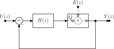
Figure 1. Simplified z-domain model of a ΔΣ converter.
Dashed lines show the additive noise model of the quantizer (Q). Y(z), U(z),
E(z) and H(z) is the z-transform of the output signal, the input signal, the
additive noise signal and the transfer function of the converter's loop filter,
respectively.
Based on this equation, it can be easily shown that if the
input signal bandwidth (B) is much smaller than the system sampling rate
(fs), and the loop filter gain is high in the band of interest
(B), while otherwise small (i.e., the filter is an integrating or
low-pass type), then in the band of interest H(z)/(1+H(z)) ~= 1 and
1/(1+H(z)) ~= 0, while at high frequencies 1/(1+H(z)) ~= 1. This
means that the output contains the input signal without any significant changes,
while the quantization noise at low frequencies is negligible, and it shows up
at higher frequencies (noise-shaping). Using adequate (low-pass) digital
filter and downsampling, the input signal with high signal to quantization noise
ratio can be reconstructed from the output signal. Since these conclusions are
derived from the linear model of a non-linear system, in the real architecture
other problems may arise (stability, quantization error with non-uniform
distribution, limit cycles, etc.), which are not addressed here.
During the research in the topic of ΔΣ A/D converters, such
analog-to-digital converter structures was sought which give optimal trade-off
between circuit complexity and conversion efficiency in a given application area
(conversion of signals with high dynamics and low frequency, e.g., pressure
sensors, weight scales, temperature measurement), and their tolerance on circuit
element mismatches is also great. The starting point of the research was the
first-order incremental converter, which was published first in 1988. This
converter is introduced briefly in the next subsection.
High Precision Incremental ΔΣ Structures
In instrumentation and measurement, there is a growing demand
for A/D converters with low or medium bandwidth, but with high absolute accuracy
(e.g., sensors, DC-measurement applications). High linearity and small offset
are also among the requirements, as well as small power-consumption and low
sensitivity to environmental noise (such as the periodic noise coupled from the
mains or digital switching noise). Manufacturing classical Nyquist-rate
converters with resolution higher than 16 bits is very expensive and requires
individual trimming. Nevertheless, Delta-Sigma A/D converters used in commercial
and professional audio or in telecommunication applications cannot deal with the
low DC-offset requirement and they usually cannot be applied for the conversion
of signals around DC.
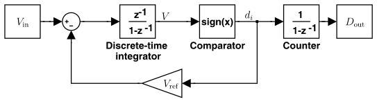
Figure 2. First-order incremental ΔΣ converter.
Vin, Vref and V is the input signal, the reference signal
and the output of the analog integrator, respectively. di is the
output of the modulator in cycle i, while Dout is the converted
digital signal at the end of the conversion.
One solution to the problem is the incremental (or
charge-balancing) ΔΣ converter, which is basically a first-order ΔΣ A/D
converter, operated in transient mode (Figure 2.). The converter represents a
hybrid between the classical dual-slope converter and the ΔΣ one. Its operation
is similar to that of the dual-slope converter, the only difference is that in a
dual-slope converter the integrations of the unknown and the reference voltages
are followed by each other, while here the two integrations are interwoven in
time. Nevertheless, the converter structure is similar to that of a first-order
ΔΣ converter, but there are significant differences in its operation: (i) the
converter operates in transient mode, up to N cycles; (ii) at the
beginning of a new conversion, both the analog and the digital memory elements
(integrators) must be reset; (iii) the digital (decimation) filter can be
realized with a much easier structure than in the case of a ΔΣ modulator.
Among the advantages of the converter is that its analog and
digital hardwares are easy to realize, there is no need of precise analog
components, its operation can be easily extended to bipolar operation even with
single reference and its area- and power-consumptions are also very moderate.
The main disadvantage of the converter is, however, that to achieve a given
resolution (nbit), the converter must be operated through
2(nbit+1) cycles, thus, its conversion rate is very
slow compared to its clock frequency.
During this research, such Δ&931; structures were sought,
which keep most of the advantages of the introduced converter, while operate
more efficiently. The research here in the lab was part of an international
project, involving a research group from Oregon State University and a design
group from Microchip Technology, Inc.
Theoretical Results
In the following the three most important theoretical result
are briefly discussed. Detailed results and derivations can be found in the
relevant publications.
Modification of the First-order Incremental Converter
One of the results of the research was the modification of the
first-order converter introduced in the previous section. The modification
involved the addition of another digital integrator to the output of the
original structure and the injection of a dither signal right before the
internal quantizer. During the research it was shown that this structure is more
efficient than the original.
The modified structure is shown in Figure 3. The novelty of the
operation is that the converter's settling time is faster due to the second
digital integrator. The error around zero, however, is not better than that of
the original structure, since the loop does not realize too small signals during
its finite operation; nevertheless, injecting dither signal into the loop forces
its feedback operation and linearizes the operation of the modulator.
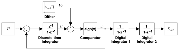
Figure 3. First-order incremental converter with second-order digital
filter and dither signal injected into the loop.
|
|
Extension of the Operation to Higher-order Loops
The most significant theoretical result is that the operation
of the first-order incremental converter has been extended to higher-order
Δ&931; loops. The main advantage of using such structures is that the
required number of cycles to achieve a given precision is much less than in the
case of first-order modulator.
Two different higher-order structure have been examined. The
first extension can be used for modulators with pure differential (or maximally
flat) noise transfer function
(NTF=(1-z-1)La), where
La is the order of the modulator) shown in Fig. 4, while
the other extension applies to modulators which have stabilized noise transfer
function (NTF=(1-z-1)La / D(z)), and are
realized by the Cascaded-Integrators, Feed-Forward (CIFF) architecture, with a
feed-forward path from the input signal to the input of the internal quantizer
(Fig. 5.). In the first case the output quantization error is bounded by
the quantization error of the internal quantizer, while in the second one the
output error is bounded by the output of the last analog integrator in the
loop.
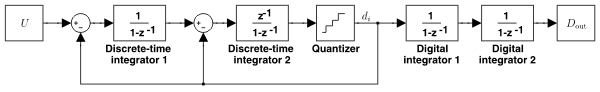
Figure 4. A possible realization of an incremental converter consists
of a second-order modulator with pure differential noise transfer function
(NTF=(1-z-1)La) and same-order digital
Cascade-of-Integrators filter.
|
|
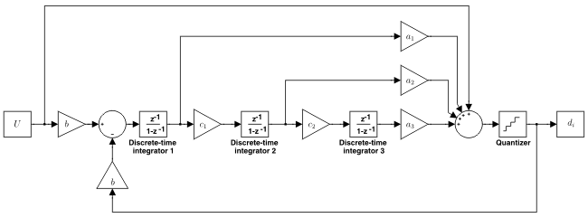
Figure 5. Third-order Cascaded-Integrators, Feed-Forward (CIFF) ΔΣ
modulator architecture, with additional feed-forward path from the input
signal to the input of the internal quantizer.
|
|
An important result is if a modulator with pure differential
noise transfer function is realized by the CIFF structure, the two extensions
become equivalent.
Design of Filters Capable of Periodic Noise Suppression
In applications of DC- or other small-frequency signal
measurements, high insensitivity to line frequency disturbances is an important
requirement. Thus, A/D converters for this area has to be able to suppress 50 or
60 Hz signals and their harmonics. The third main result of this research was
the design metodology of optimal higher-order digital sinc-filters for
higher-order incremental ΔΣ converters for suppression of periodic noise
disturbances.
Practical Results
The theoretical results discussed above briefly has been
utilized in a design co-operation between Oregon State University and Microchip
Technology, Inc. Based on the achieved results, a 22-bit DC-measuring A/D
converter has been designed and fabricated. Another fruit of the co-operation
was a circuit-level implementation patent.
Related Publications:
|
J. Mįrkus, J. Silva, and G. C. Temes,"Delta-sigma architectures for dc measurement - an
overview," in CICC'2006, Proceedings of the IEEE 2006
Custom Integrated Circuits Conference, San Jose, CA, USA,
10-13 Sept. 2006. |
A tutorial paper about the evolution of incremental converters. Brief
discussion of the theoretical derivations and implementation difficulties,
and a short summary of the measurement results of the manufactured 22-bit
converter. |
|
J. Mįrkus, Higher-order incremental delta-sigma analog-to-digital
converters, Ph.D.thesis, Budapest University of Technology
and Economics, Department of Measurement and Information
Systems, Budapest, Hungary, Mar. 2005, 132 p. |
Ph.D. thesis containing the results. The most detailed work on the
topic of incremental converters. It contains detailed theoretical
derivations (calculation of the required number of cycles for a given
resolution, signal-to-noise ratio of the converter, comparison of
different architectures). Examination of non-ideal effects (noise,
non-linearity of op-amps, finite gain, etc.). Digital filter design for
incremental converters. Complex design examples. |
|
J. Mįrkus, J. Silva, and G. C. Temes, "Theory and applications of incremental delta-sigma
converters," IEEE Transactions on Circuits and Systems-I:
Regular Papers, vol. 51, no. 4, pp. 678-690, Apr.
2004. |
Extension of the operation of the first-order converters to
higher-order modulators. Derivation of the required number of cycles for a
given resolution. Application of dither signal to improve the efficiency
of the first-order converter. Sinc-filter design to suppress periodic
noise. |
Further publications on A/D converters can be downloaded from here.
Useful links
Further information: Jįnos Mįrkus
|